01. CUDA C Basics
-
Host: The CPU and its memory -
Device: The GPU and its memory
Simple Processing Flow

-
COPYmemory (from CPU to GPU) -
LoadGPU program andExecute -
COPYmemory (from GPU to CPU) Free
Problem::vector addition

- 1:1 (input:output)
Concepts
__global void mykernel(void) {};

mykernel<<<N,1>>>(); // Grid (N blocks), Block(1 thread)
-
__global__is kernel code (run in device) -
<<<GRID, Block>>>, which means- GRID: # of blocks per grid
- Block: # of threads per block
// 1-1. prepare gpu's global memory
cudaMalloc((void **)&d_a, size);

// 1-2. copy (to device A from host A)
cudaMemcpy(d_a, a, size, cudaMemcpyHostToDevice);

// 2. Load and Execute
add<<<N,1>>>(d_a, d_b, d_c)

// 3. Copy (GPU -> CPU)
cudaMemcpy(c, d_c, size, cudaMemcpyDeviceToHost);

// 4. Free
free(a);cudaFree(d_a);
02. Shared Memory
Problem::1D Stencil

- It is not an 1:1 (input: ouput) problem.
- e.g. blue element is read seven times (if radius 3)

Concept::Shared Memory

- On Chip memory (>= Global memory)
- Per Block (invisible other blocks)
- User managed memory
__shared__ int s[64];
...
Starting from Volta (2017 and later),
__shared__(SW) and the L1 cache(SW) share the same on-chip SRAM(HW) resources. Developers can configure how much of this SRAM is allocated to shared memory versus L1 cache depending on the application needs.
03. CUDA Optimization (1 of 2)
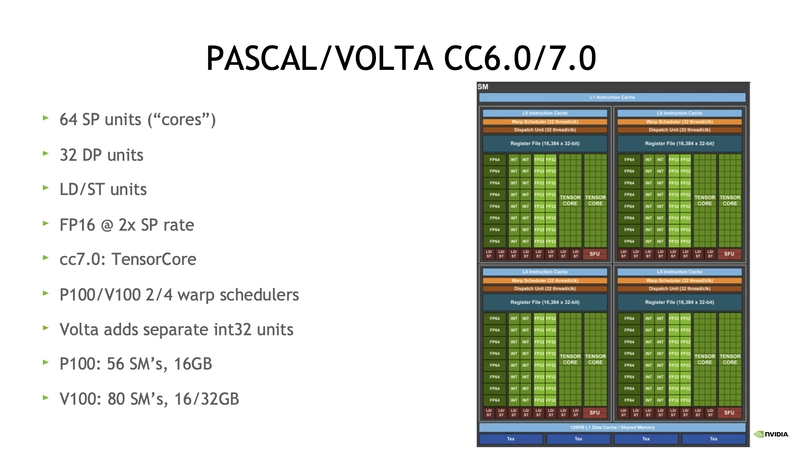
Architectures
- Tesla -> Fermi -> Kepler -> Maxwell -> Pascal -> Volta(2017) -> Turing -> Ampere -> Hopper(2022) -> Ada -> Blackwell(2024)
-
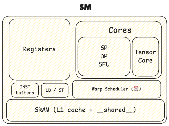
CC: Compute Capability -
GK110: Chip name -
SMX,SMM: Enhanced SM - Processors
- SP: Scalar Processor (ALU, FP32)
- DP: Double Precision Unit (ALU, FP64)
- SFU: Special Function Unit (sin, cos ...)
- Tensor Core: Matrix mul
- INT
- LD / ST: Load / Store Unit
- Tensor Cores: for matrix multiplicaiton
Warp scheduler
Each warp scheduler is dual issue capable
dual issue capable: It can issue and execute two instructions simultaneously in a single clock cycle
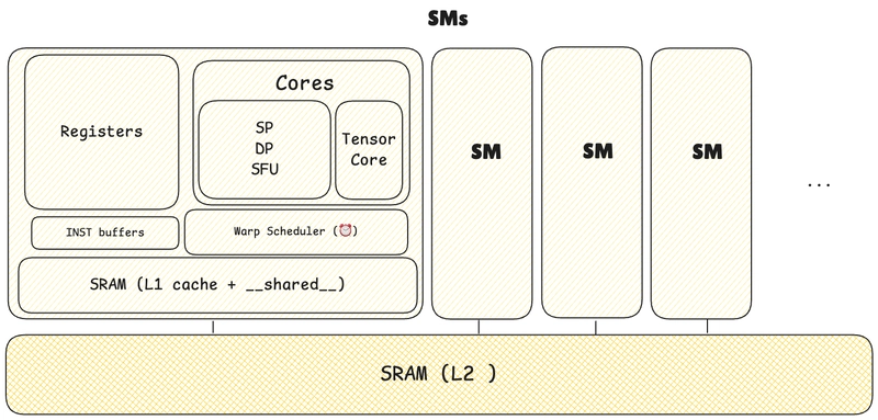
Execution Model
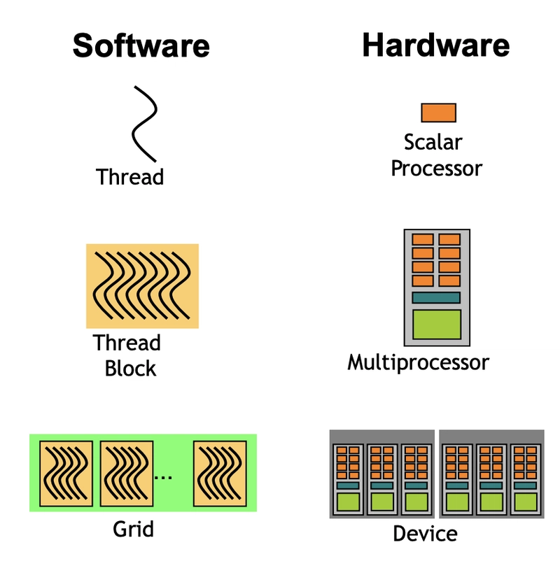
- Scalar Processor: SP / DP / Tensorcore ...
- Multi-Processor:
SM(Streaming Multiprocessors)
Multiple threads in a thread block are not (never) spread across different SMs.
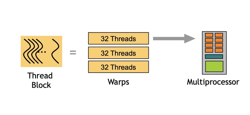
1 Block(SW) --> N Warps(HW) --> 1 SM(HW)
For example, 1024 tasks and if BLOCK_SIZE is 1024 would create 32 warps (1024 / 32), all of which must execute on the same SM. This can create bottlenecks.
Once threads begin execution on an SM, they cannot migrate to a different SM. They must complete execution on their assigned SM.
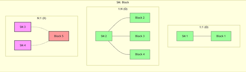
- 1 block :1 SM (ok)
- N block :1 SM (ok)
- 1 block :N SM (x)
Launch Configuration
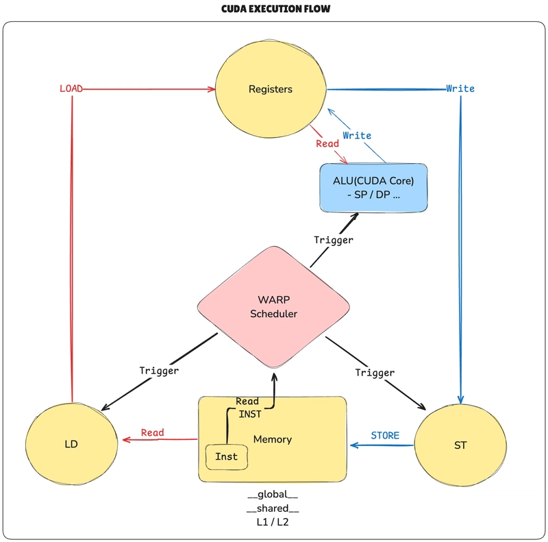
- Instructions are issued in order
-
Thread Stall: A thread stalls when one of the operands isn’t ready -
Latency hiding: Hide latency by thread Context switching
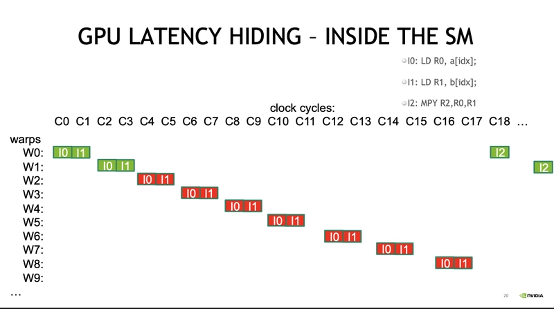
CUDA need enough threads to hide latency
Since CUDA uses SIMT, each warp can be in a different instruction execution state.
-> Also CUDA processes instructions in-order
-> if data isn't ready (e.g. LD memory -> register), operations like SP, DP, MPY(multiply) cannot execute, leading to a thread stall.
-> To prevent idle cycle(wastage), context switching is performed at the warp level to hide latency (latency hiding)
Conclusion
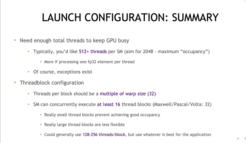
- Launch enough
threadsper SM to hide latency - Launch enough
threadblocksto load the GPU
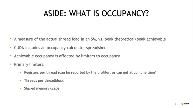
Occupancy= Active warps / Maximum number of warps per SM
It represents how efficiently the GPU’s Streaming Multiprocessors (SMs) are utilized.
An occupancy of 1.0 (or 100%) indicates the SM is working at full capacity.
04. CUDA Optimization (2 of 2)
Memory OP
Memory operations are issued per warp (LD, ST, 32 threads in parallel), just like all other instructions.
Even if only 4 bytes are needed (e.g., for int or float), global memory requires a 32-byte segment, while fetching from the cache requires loading a 128-byte line.
| Property | Line | Segment |
|---|---|---|
| Size | 128 bytes | 32 bytes |
| For Cache | Yes (Used in L1, L2 cache) | No |
| For Global Mem | No | Yes (Used in global memory) |
| Hardware | SRAM (Static RAM) | S-DRAM (Synchronous Dynamic RAM) |
Coalescing
Coalescing happens when a warp (32 threads) needs data from multiple memory addresses, and those addresses are grouped together in a single chunk (e.g., 0, 4, 8, ..., 124). The GPU can fetch this chunk in one go, making it efficient.
If the addresses are scattered (e.g., 0, 100, 500), the GPU has to fetch multiple chunks, which is slower and less efficient.
Bus Utilization
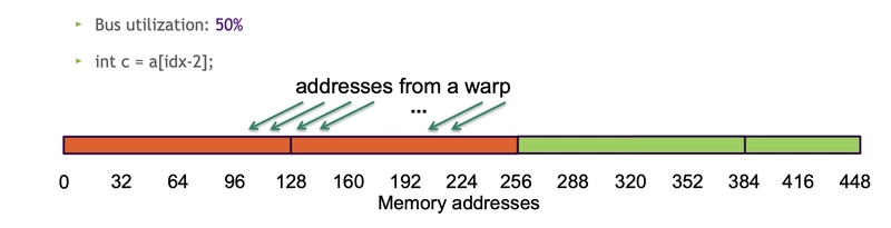
c = a[idx] // idx = global thread idx
In a single operation, 32 warps × 4 bytes = 128 bytes are needed. Ideally, this can all be fetched with one cache line (128 bytes).
- Bus utilization: 100%
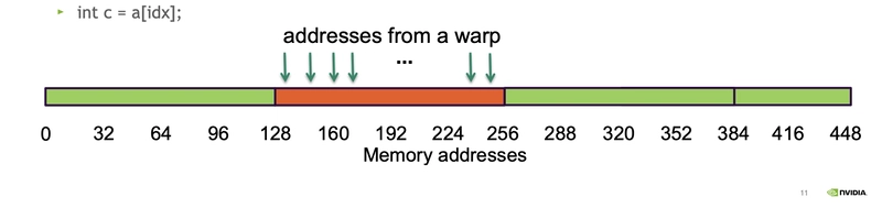
This achieves 100% bus utilization (ideal coalescing), meaning no bytes are wasted. (Typically, waste occurs due to the minimum size imposed by line or segment fetches.)
- Bus utilization: 50%
c = a[idx-2]
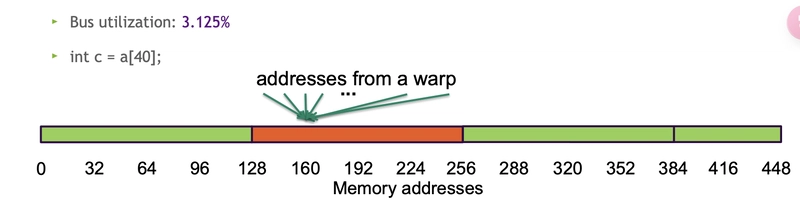
- Bus utilization: 3.125%
c = a[40];
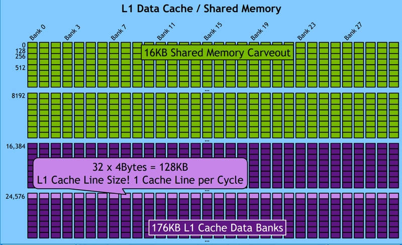
Shared Memory Optimization in CUDA
- Purpose: Allows threads within a block to communicate and share data.
- Structure: Divided into 32 banks, each 4 bytes wide.
- Bandwidth: Typically 4 bytes per bank per 1-2 clock cycles per multiprocessor.
- Access Pattern: Shared memory accesses are issued per warp (32 threads).
Memory Bank Explained: A bank is a hardware unit in shared memory (SMEM) that splits data across multiple memory chips for parallel load/store operations. This increases bandwidth and reduces contention. In contrast, cache uses "lines," and global memory (SDRAM) uses "segments."
-
Bank Layout: In CUDA, shared memory has 32 parallel banks. For example, if
__shared__memory is 64KB, it’s split across 32 banks (2KB per bank). - Access: Each bank can serve 4 bytes per cycle in parallel.
Code
__global__ void kernel(float* in, float* out, int n) {
    __shared__ float s_data[256]; // 256 floats = 1KB, split across 32 banks
    int idx = threadIdx.x + blockIdx.x * blockDim.x;
    if (threadIdx.x < 256 && idx < n) {
        s_data[threadIdx.x] = in[idx]; // Each thread loads to a bank
    }
    __syncthreads();
    if (idx < n) out[idx] = s_data[threadIdx.x];
}
// Launch: kernel<<<(n+255)/256, 256>>>(in, out, n);
Bank Access Details
- Single Precision (4 bytes): A warp (32 threads) reading 4-byte floats = 128 bytes (32 × 4). Matches a 128-byte cache line, so it takes 1 cycle if aligned and contention-free.
- Double Precision (8 bytes): A warp reading 8-byte doubles = 256 bytes (32 × 8). If the GPU fetches 128 bytes per cycle, it needs 2 cycles to get all 256 bytes.
Bank Conflicts
- What It Is: When a warp’s 32 threads try to access the same bank, causing serialized reads (multiple cycles).
-
Example (FP32 Array):
- Assume a
__shared__array of 32 floats (128 bytes) stored across banks 0–31. - If each float is 4 bytes and continuous, banks 0–31 hold the first 128 bytes (32 floats).
- Problem: If threads need more than 4 bytes from the same bank (e.g., misaligned doubles), a bank conflict occurs, slowing it down.
- Assume a
- Impact: For an FP32 array, fetching all 32 elements in one cycle fails if alignment or bank access overlaps (e.g., FP32 array[16] takes 2 cycles due to bank contention).
Avoiding Bank Conflicts
- Tip: Ensure each of the 32 threads accesses a unique bank.
- Code Fix:
  __shared__ float s_data[32]; // 32 floats, one per bank
  int tid = threadIdx.x;
  s_data[tid] = in[tid]; // Each thread hits a different bank
  __syncthreads();
  out[tid] = s_data[tid];
- Alignment: Pad data if needed to avoid overlap (e.g., use 32-wide arrays).


Top comments (0)