
- We will talk about the working of depletion MOSFETs now in general .Here are a few important features to remember which would help you out later on,
- They are commonly known as Switched On devices.
- In depletion mode, the width of the channel is dependent on the gate voltage.
- If the applied gate voltage is positive then the channel width would eventually increase, as we discussed earlier.
- On the other hand, if a negative voltage is applied to the gate, the width of the channel decreases, and hence the drain Current ID also decreases.
- If the negative voltage is much higher in value, then the MOSFET shifts into the cut-off region.
- MOSFET characteristics vaires from a normal FET, short for field effect transistor.
I-V characteristics of Depletion mode MOSFET
Here is a brief overview that how is it done, we will discuss both the types later in this section;
- The V-I characteristics of depletion-mode MOSFET are plotted between the varying values drain-source voltage represented by VDS, with the Drain current ID.
- Initially, a little amount of gate voltage produces a small drain current represented in the Ohmic region of the graph.
- As the value of positive voltage increases, the value of drain current also increases and reaches the maximal potential of the MOSFET, this region is labeled as Saturated or Active Region.
- In the case of applying a negative voltage to the gate, we would get a sharp decline in the value of Drain Current ID as you can see from the graph.
I-V characteristics of N channel depletion type MOSFET
- Let us discuss the current transfer characteristics of the N channel depletion types MOSFET with the help of a characteristic curve plotted between the drain to source voltage VDS and drain to source current represented by IDS.
- Refer to the graph given below for better understanding:
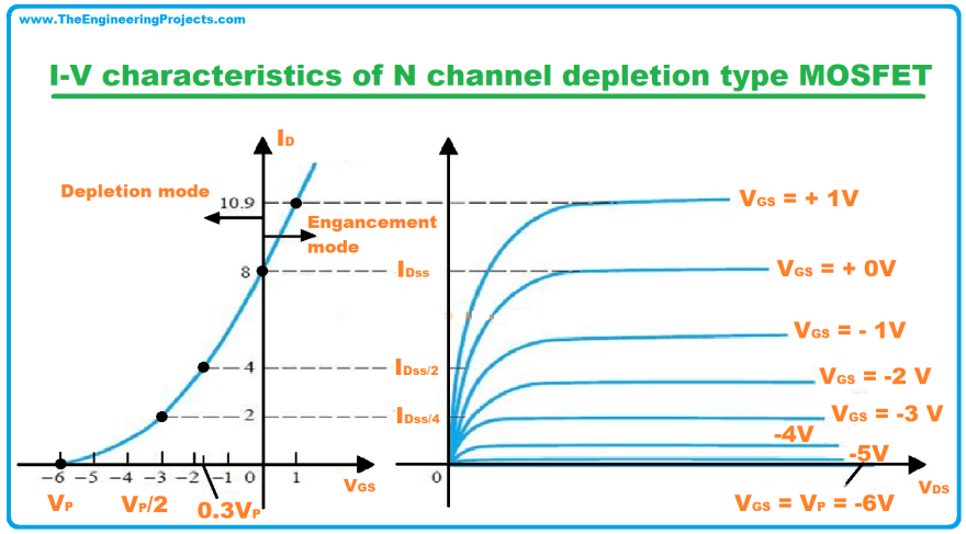
You can observe from the graph that a little amount of current is still flowing through the N channel depletion type MOSFET even when the VGS is zero. This is represented by the cut-off region of our graph. Mathematically we can summarize it as; VGS < -VT
- In the next phase the current IDS starts increasing with the increasing value of VDS, this phenomenon can be observed in the Ohmic region of the graph. The mathematical expression can be written as: VGS > -VT and VDS < VP
- After the Ohmic region, there is the saturated region of our graph, by now you must be aware of what is happening in this region? If not, let me solve it for you, N channel depletion type MOSFET operates in the saturated region when the VDS reaches a certain value of voltage called Pinch off voltage. Pinch-off voltage is represented by VP. After reaching the pinch-off voltage our n channel MOSFET passes the saturated current.
- It is evident from the graph that, the value of VP and IDS would increase with the increasing value of VGS. We can summarize the whole scenario as ; VGS > -VT and VDS > VP
- Here a question arises, what would you do if you want to operate your N channel depletion mode MOSFET in the cut-off state? The answer to this question is simple, make your VGS which the gate to source voltage negative, and voila you are done!
- At the point at which the VGS reaches the negative voltage level of -VT, IDS would become Zero, no IDS means no channel leading to no conduction!
I-V characteristics of P channel depletion type MOSFET
- P channel depletion type MOSFET has majority charge carriers in the form of holes, the characteristic curve is plotted between the VGS which is the Gate to source voltage, and current IDS, which is the drain to source current.
- Refer to the graph given below for better understanding:
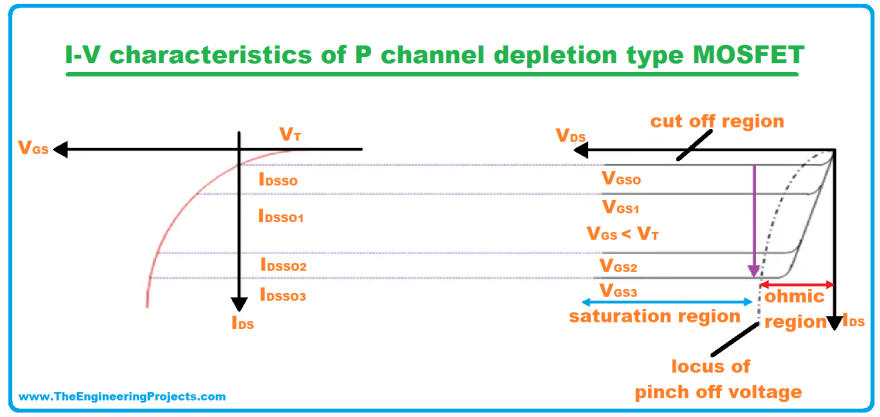
- By default, we have the conduction channel already established to an extent in P channel depletion type MOSFET so the current IDS is not zero even when the voltage VDS is zero. This is represented in the cut-off region of our graph. In this case : VGS > VT
- The value of current represented by IDS increase with the value of VDS, refer to the Ohmic region of our graph, refer to the graph for a better understanding. We can summarize that: VGS < VT and VDS > -VP
- Afterward, when the VDS reaches a certain maximal pinch-off voltage VP, P channel depletion type MOSFET starts operating in the Saturated region. We can summarize the whole process by writing the following expression: VGS < VT and VDS < -VP
- The saturated current increases with the negatively increasing value of VDS, Follow the values of IDSS, from IDSS1 to IDSS3 with the values of VGSO to the values of VGS3, can you figure out the pattern?
- When VGS is equal or greater than the threshold voltage VT, then at this point, the P channel depletion type MOSFET would lose its conduction channel reaching the pinch-off voltage, this would, in turn, leave the P channel depletion type MOSFET again into the cut off region switching off the device.
- So, this was the last segment for the characteristics of our MOSFET, let us move to the final notes to conclude this discussion.


Top comments (0)