
Hi there! Glad to see you. Thank you for stopping by. In today’s post, I’ll be covering BJT (Bipolar Junction Transistor) in detail.
BJTs are commonly used in electronic circuits as an amplifier, oscillator, rectifier, filter, and even as a switch. BJTs are bipolar electronic devices that use both electrons and holes as charge carriers.
Curious to know more about BJTs?
Stay connected.
BJT Definition:
The BJT(bipolar junction transistor) is a three-terminal semiconductor electronic device mainly used for switching and amplification applications. The three terminals are named: emitter, base, and collector. In BJTs, the large current at the collector and emitter sides is controlled by the small input current at the base terminal. Earlier, germanium was used for the development of BJTs, while recent BJTs are composed of silicon material.
BJT Symbol:
The BJT is divided into two main types: NPN and PNP and symbols of both transistors are shown below.
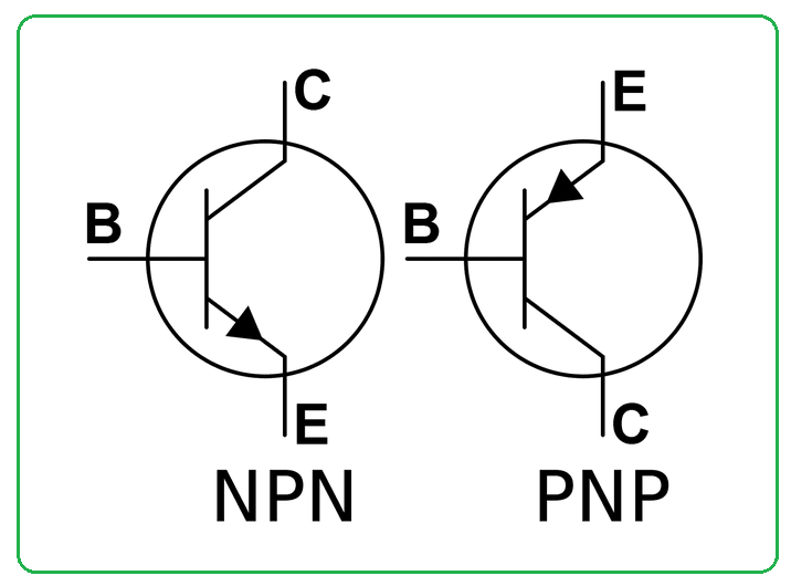
The direction of the current flow in symbols is represented by the arrows. Current flow will occur from emitter to base side in PNP transistor and from base to emitter side in NPN transistor.
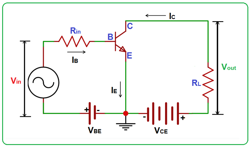
BJT Working:
The base pin is responsible for the working of the entire device. The voltage at the base pin will turn ON the NPN transistor and current flow will occur from the collector to the emitter pins. This current flow is denoted by Ic and is called collector current. In an NPN transistor, there are two junctions: one is a base-emitter junction that is forward-biased and the other is a collector-base junction that is reverse-biased.

The depletion region width at the base-emitter junction side is less than the depletion region width of the collector-base junction. The base-emitter junction is forward biased and the potential barrier is decreased at this junction which will cause the electron flow from the emitter to the base side.
The electrons at the base region are not held there for the maximum time since the base side is very thin and lightly doped. These electrons will make pairs with the holes available at the base side and as a result, they flow out of the base side in the form of base current. The leftover electrons that don’t get attached to the holes at the base region then enter the collector region as a collector current.
Based on Kirchoff’s Current Law, when we add both base current and collector current, they will be equal to emitter current.
Ie = Ib + Ic
This is how the NPN transistor works. The working of the PNP transistor is similar to the NPN transistor but holes are majority carriers in the PNP transistor and the current flow will occur from emitter to collector pins.
BJT Characteristics:
All there pins of the BJT device come with different doping concentrations. The base side is thin and lightly doped and the emitter side is highly doped while the collector terminal is moderately doped.
There are three different configurations to connect BJT devices:
- Common-base configuration
- Common-emitter configuration
- Common-collector configuration
We’ll study each one by one.
A: Common-base configuration
In this configuration, the base pin is kept common between the input and output signals.

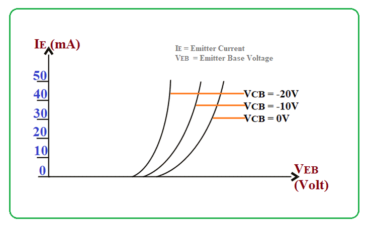
The characteristics of the BJT can be best explained by the V-I curve. In the following curve, we’ll take base-emitter voltage Vbe on the x-axis, and emitter current Ie is taken on the y-axis
The following figure shows the output curve of the common base configuration where collector-base voltage Vcb is taken on the x-axis and the collector current Ic is taken on the y-axis.
The characteristics curve exhibits three different regions called the cutoff region, saturation region, and active region. Both emitter and collector junctions are reverse biased in the cutoff region, and both emitter and collector junctions are forward biased in the saturation region and the emitter junction is reverse biased in the active region.
B: Common-emitter configuration
In this configuration, the emitter terminal is kept common between the input and output signals.
The following graph shows the input characteristics curve of the common-emitter configuration where base-emitter voltage Vbe is kept on the x-axis and the base current is taken on the y-axis.
The collector-emitter voltage Vce on the x-axis and the collector current on the y-axis shows the output characteristics curve of the common-emitter configuration which, similar to the common-base configuration, carries three regions. Both collector and emitter junctions are forward biased in the saturation region, while emitter junction is not fully reverse biased and collector current is not fully cut off in the cutoff region. And the collector junction is reverse biased and the emitter junction is forward biased in the active region.
C: Common-collector configuration
This configuration is also called voltage follower circuit where collector terminal is kept common between input and output signals.
In this configuration, the input impedance is high and is mainly used in impedance matching circuits.
BJT Types:
BJT are divided into two basic types:
- NPN Transistor
- PNP Transistor
Let’s study each one by one.
1: NPN Transistor
NPN transistor belongs to the BJT family where two N-doped layers surround the one P-doped layer. The base terminal is the middle P-layer while the other two N-layers show the collector and emitter pins. In NPN transistors, both electrons and holes take part in the conduction process, but holes are minor carriers in this case while electrons are the major carriers. The applied voltage at the base side will bias the device and as a result, the current flow will occur from the collector to the emitter pins.
2: PNP Transistor
PNP transistor belongs to the BJT family where two P-doped layers surround the one N-doped layer. The base pin is represented by the N-layer while collector and emitter pins are represented by two P-doped layers. Again, both electrons and holes take part in the conduction process in the PNP transistor, but electrons are the minor carriers and holes are the major carriers. The voltage at the base pin will bias the device and the current flow will occur from the emitter to collector pins.
Know that the mobility of electrons is better and faster than the mobility of holes, the reason NPN transistors stay ahead over PNP transistors for their usage in electrical circuits.
BJT Applications:
- BJTs are commonly employed for amplification and switching purposes.
- BJTs carry high voltage gain and low forward drop voltage; the reason they are the right match for voltage, current and audio amplification applications.
That’s all BJTs. Hope you’ve found this article useful. You can approach me in the section below if you’re unclear about anything. I’ll try my best to help you out. Thank you for your precious time.


Top comments (1)
Excellent article 👍