Hello everyone and welcome to this article. We are going to have a look at the evolutions that have taken place in the area of the printed circuit boards from generation to generation. Since the discovery of the printed circuit boards (PCB), we have witnessed a lot of positive changes in the size, shape, material and functions in this area. There have been so many significant changes that have taken place in this area which have positive impacts in the area of electronics and the technology at large.
Previously, we have noted that the printed circuit board is the backbone that provides the surface for mounting electrical circuits and electronic components. This circuits find their use in almost everything that involves electricity such as computers, laptops, cell phones, televisions, radios and many more.
For us to have a better understanding of the printed circuit boards and how far this technology have come, let us have a look at the evolution of the printed circuit boards:

The PCBs early years
The earliest printed circuit board can be traced back in the early 1920s. the PCB could use almost any type of material as the base material and this included even wood. Holes were drilled into the material the wires were inserted in the holes. Funny enough is that instead of the use of the rivets, nuts and bolts were used. For a modern technologist, I know you can’t believe especially when you do a comparison with the modern PCBs, but actually, this concept worked and here is where the PCB technology started. It is this time, there was no much demand of the printed circuit boards. The only two applications that needed the PCBs were the radios and the gramophones.
Charles Ducas patented the first PCB in 1925 dabbed as the ‘printed wire’ which involved the printing of the circuit directly on an insulated surface. While this process eliminated the need of the complex wiring of the printed circuit board, it was not the case until in 1943 when Dr. Paul Eisler an Austrian made the first operational printed circuit board.

World war II
1947 welcomed production of the double-sided PCBs. The unique method involved the use of the through-hole plating which could allow the designers to use both sides of the PCB. The copper plating that was done on both sides of the PCB allowed the flow of the electricity on both sides of the printed circuit board.
1949 the United States of America Army Members, Moe Abramson and Stanislaus F. Danko developed the first auto-assembly process and this changed drastically the way printed circuit boards were being made. Here, copper foil interconnection pattern and the was used. The dip soldering technology was also introduced for the inserting of the component leads onto this boards. developers drew the wiring diagram then made a photograph of it on zinc plate then created a printing plate using the zinc plate for an offset printing press.
The circuit board development.
From 1920s it took at least 30 years before the PCB manufacturing process was done using specific resins and suitable materials. In the 1947s and 1960s single sided and double-sided PCBs became popular where by the components were placed on one side while the circuitry was placed on the other side. This was a great improvement as compared to the bulky wiring circuitry that had been previously used. In 1957, Moe Abramson and Stanislaus F. Danko patented their method. The same period of 1960s, the US introduced the process of soldering the printed circuit boards which further improved the PCBs quality. The process involved making a drawing of the wiring diagram or pattern and then photographing it on a zinc plate and this could be used later as the printing plate. This was a very significant breakthrough that let to great improvement on how the printed circuit boards were made.
In the late 1960s, the printed circuit boards began to be built with more advanced techniques and technology which improved on how circuits traces and components could be protected from the corrosion and damages. This is the same period where multilayer PCB were introduced and their production initiated. In the 1970s, the PCB circuitry and their components sizes started to get smaller hence making the boards that were produced much smaller. This is the period where hot air soldering method came into use in the area of the PCB production.
Complexity and the miniaturization
1980s came with more advanced changes in the area of the PCB manufacturing. This is the period where the surface mount technology came in hence leading to much more reduction in size of the printed circuit boards. The surface mount technology became very poplar replacing the through hole technology because the components that were used were very small and could reduce the size of the board by occupying very less space but still maintain the same functionality that was offered by the previous technology.
In 1990s, there was introduction of the computer aided manufacturing which came in with a lot of advantages to the PCB development. This increased the complexity of the circuit boards that were being manufactured to another significant level. The technology allowed flexibility of the boards and allowed them to be adaptive to various applications. While the complexity of the PCBs keeps growing, the cost has always remained low and affordable.
1995 welcomed another advanced PCB manufacturing, the high density-interconnector PCBs. This type of boards feature, small vias, pads and traces and provide very significant benefits such as small size and less weight. From this point, the traditional boards came outdated. The rigid-flex PCB became very common and affordable.
The digital Age
This period came in in 1980s and it played a very great role on how consumers viewed the electronics industry. At this period, the demand of the electronic gadgets in the United State was growing at an alarming rate. The electronic vendors were having a hard time to maintain the supply chain and keep the shelves filled with the stocks. Electronics gadgets such as the cameras, the DVD players, portable radios and the gaming console could not last in shops due to this high demand. As demand for these electronics went high, the demand for more smaller and compact printed circuit boards went high too.
This made developers to go back to drawing board and try to figure out on how they can solve the challenge of the market demand. Out of hard work, they came up with the surface mount technology and because of the reduced size, reduced cost of production and affordability of this boards, the surface mount technology became the most popular method as compared to the through-hole technology method.
At this same period, engineers and designers wee still using their hands and stencils to draw the circuit. However, the introduction of the computers and electronic designs (electronic design automation- EDA) software in the mid 1980 made manufacturers to switch to digital design. The advancement in the electronic software made massive improvement on how the PCBs were being manufactured and also saved the industry countless hours due to fastened production.
The 1990s
Apart from making greater moves in the complexity of the printed circuit boards, the cost of production of the same decreased drastically in the 1990s. This was advantageous to the manufacturers as it made them increase the quantity and quality of the electronics that they made in order to meet the demand that was increasing on a day-to-day basis.
In the 90s, the use of the silicon became so popular especially with the ball grid array packaging method, that is used for the integrated circuit-IC packaging. The type of packaging provides a more interconnecting pins than the other methods such as the dual in line packaging. Instead of using only the perimeter, the entire bottom surface of component could be used for pins.
In the 1990s, there were no much changes made on the PCB but we must take note that the design process begun to change. The developers shifted their focus on the IC design and designs for test strategies were introduced into the layout. Instead of coming up with a one-time use design, the developers started coming up with PCB designs with a mind of future reuse. This is the period where there was separation between the designers and the manufacturers.
In the year 1995, the PCB manufacturing reached a market value of 7,5 billion USDs. This is the same year where the micro via technology was introduced in the PCB manufacturing.
The internet Age
The period of 2000s, the printed circuit boards became even more smaller and complex but the flexible printed ones became more common. The boards provided a flexible and affordable option where space was a greater concern. The flexible printed circuit boards offered wide range of the motion making it possible to apply them in both bend -to install and dynamic options.
2006, developers came up with Every Layer Interconnect (ELIC) process which employed the use of the stacked copper micro-vias in order to create the connection between different layers of the printed circuit board. Although the process was good for the flexibility of the PCBs, the technology was not used until in the late 2010.
The Modern Day PCBs
While a printed circuit board could have around 30 transistors, the modern day printed circuit boards might have millions of the transistors in a single chip called integrated circuit. This is courtesy to the changing techniques and technologies that have enabled more changes in the area of the printed circuit boards. by the shrinking of the components such as the capacitors, diodes, inductors, transformers, resistors and the transistors, the developers can now produce high density boards and achieve great flexibility.
As the components have gotten smaller and complex, the assembly of the printed circuit boards by the use of hands has become impossible. Today, the components have become so microscopic and to achieve the required production, machines are used. It is the shift in complexity that have triggered electronic manufacturing optimization.
Machines in the PCB production area.
Below is a list of machines that have evolved the PCB manufacturing industry;
-
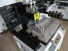
PCB drilling machine; even though we have said that the SMD are mounted on the surfaces, remember that there need to be connection between layers of the PCB boards. this is done via vias which are very tiny holes drilled on the board. This is done by the use of the drilling machine.

-
Wave soldering machine; this is used for the soldering process. It is also very important in the mass production of the boards.

-
The PCB brushing machine; we have talked about via drilling. Now after the drilling process is done, we have debris that are deposited. These debris are removed by the PCB brushing machine.

-
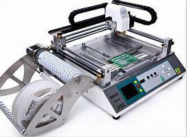
Pick and place machine; this picks the components, rotates them to the required direction and place them on the PCB board I preparation for the components solder.
-
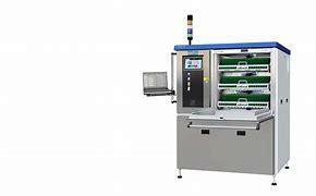
The PCB cleaning machine; this does all the necessary cleaning that is required on the board. It also ensures that the board is very dry and free from any form of moisture.
-
Solder paste printing machine; this is for printing the solder paste to attaches the components on the board. It ensures that the process is easy and first.
-
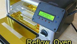
Reflow oven; this does the actual soldering of the boards.it ensures that the process is done in an effective way. We have three types that are currently common in the market; vapor phase oven, infrared oven and the convection oven.


Top comments (0)